RP2040 Industrial I/O Board
Continuing my work at Harsch Systems, I designed two generations of an RP2040 industrial I/O board in KiCad, with 0–10 V and 4–20 mA input and output, along with optical isolation.
- When
- 2021
- Status
- Completed
- Role
- Engineering Intern, Harsch Systems
Overview
In my first project at Harsch Systems, I had worked on device drivers to meet strict timing constraints for industrial applications. Next, my boss wanted to see if we could build our own architecture to cut costs and improve our system control.
In this project, I designed a board around the Raspberry Pi RP2040 microcontroller. The industrial systems we were looking at commonly worked with 0–10 V and 4–20 mA signals, none of which a 3.3 V microcontroller can handle directly. This board enables that control for the digital processor. I designed it twice: first as a through-hole carrier for a Raspberry Pi Pico module, then as a compact surface-mount board built around the bare RP2040 chip.
Circuit Design
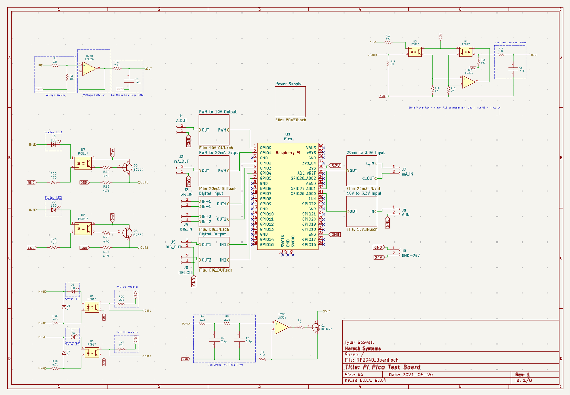
First, I had to learn a little more about circuit design. My boss had an additional requirement that he wanted optically isolated inputs (using PC817 optocouplers), and built-in filters for analog control. Before doing any design, I prototyped the following subsystems:
- Analog outputs: the Pico’s PWM outputs were smoothed by active low-pass filters and scaled by LM324 op-amp stages into a 0–10 V output or a 4–20 mA current output.
- Analog inputs: a voltage divider, voltage follower and low-pass filter took 0–10 V signals down to the ADC’s 3.3 V range. A stage to convert the 4–20 mA input to a voltage was designed as well.
- Digital I/O: inputs and outputs were optically isolated with PC817 optocouplers, with BC337 transistor drivers on the outputs and status LEDs on every channel.
- Power: the board ran from a separate 24 V supply.
PCB Version 1
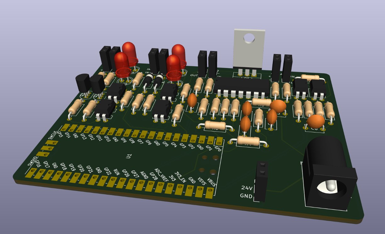
Once I had these working on a breadboard, I moved into the PCB design portion of the project. This involved taking the exact same subsystems from before and integrating them with the Pico into one larger PCB structure.
PCB Version 2
The second version dropped the whole Pico module and put the RP2040 chip directly on the board. This meant designing the support circuitry the Pico normally provides, such as QSPI flash, a crystal for the clock, a TPS56339 switching regulator for power, USB for programming, and I2C connectors for auxiliary sensors.
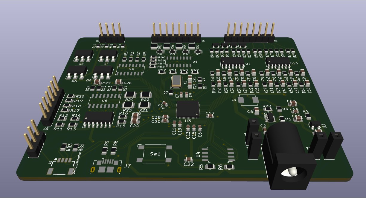
The final designed board is shown below. Moving to surface-mount parts made it far more compact.
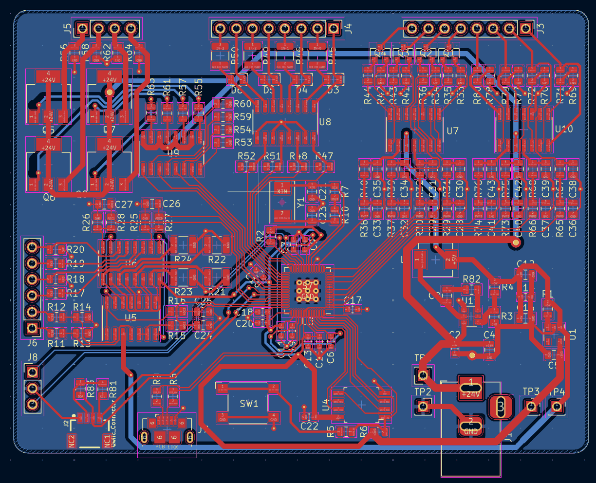 The final version layout in KiCad. Signal traces fan out from the RP2040 at the center, the wide traces on the right carry power from the 24 V input, and the analog and digital I/O circuits line the connectors along the edges. Click to enlarge.
I was unable to test the final board before I left, but I gave my boss good documentation and all the associated files to enable a prototype to be built in the future. This was the first time I designed a PCB, and I’m super grateful for the support I received and the work I could accomplish.