Semiconductor Device Fabrication in the Cleanroom
On a team of four in BYU's cleanroom, I helped fabricate our own semiconductor devices from scratch, including a MOSFET, photodiodes, solar cells and a laser.
- When
- 2026
- Status
- Completed
- Role
- Team Member
- With
- Team of 4
Overview
This was another class project that I had to include here. Actually, I didn’t even have to take this class for my major. The second half of it, I had to request an add code for, and it didn’t count towards my graduation. However, I had heard about this class and determined that it was one of the most interesting classes at BYU, so I took it just to learn more.
Over two semesters, I worked with a team of four in BYU’s cleanroom to fabricate semiconductor devices, including a MOSFET, LED, photodiode, and laser. I want to show some of the results from a few of those projects here!
MOSFET
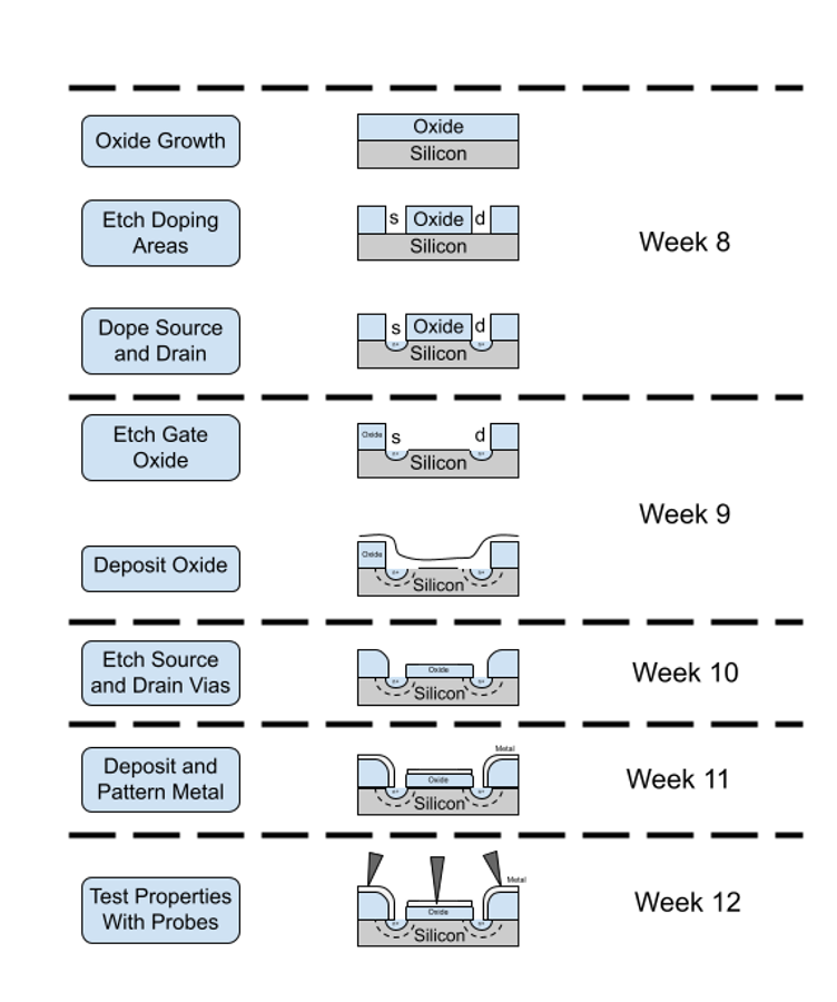
This class taught me a lot about how semiconductor devices work, both on the theoretical and experimental side. Our first-semester target was to create a MOSFET on silicon: growing an oxide, etching and doping the source and drain, etching back to form the gate oxide, opening vias, and depositing and patterning the metal contacts. We had a set of premade masks available to us and full access to the cleanroom to make it happen.
Our MOSFETs were likely the most successful in the class! The I–V curves were near ideal (with some channel length modulation higher than expected given the device parameters).
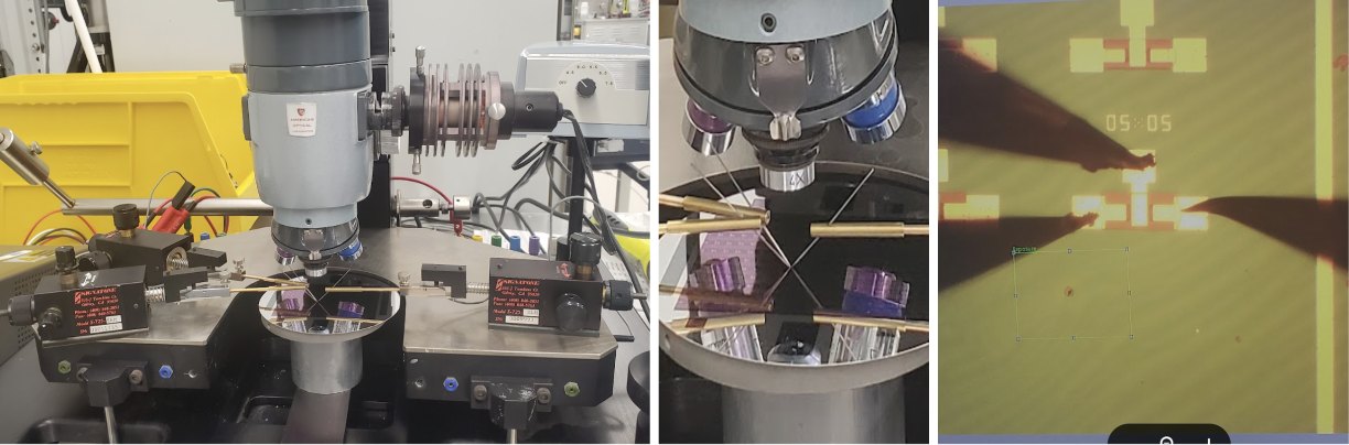 Testing the finished transistors on a probe station (left), with the probe tips on the wafer (center) and landed on a device’s contact pads under the microscope (right).
Photodiodes
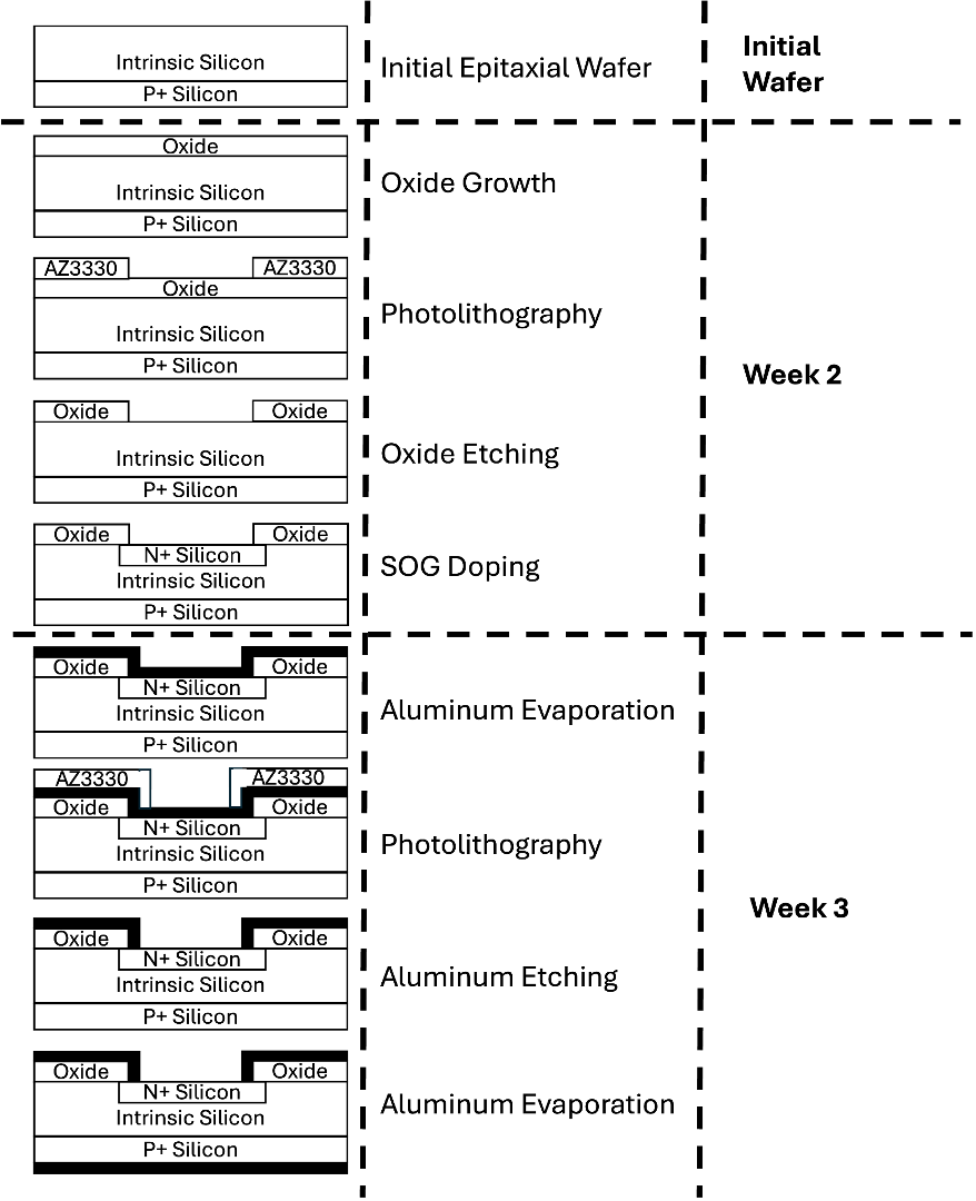
The photodiodes started from an epitaxial wafer with an intrinsic silicon layer on P+ silicon. We grew an oxide, patterned it with photolithography, doped an N+ region with spin-on glass, then evaporated and patterned aluminum contacts on the front and back.
The photodiodes worked well! Our quantum efficiencies were not particularly high (though our measurement setup was also not particularly precise), but they were able to detect fairly low light levels from a distance.
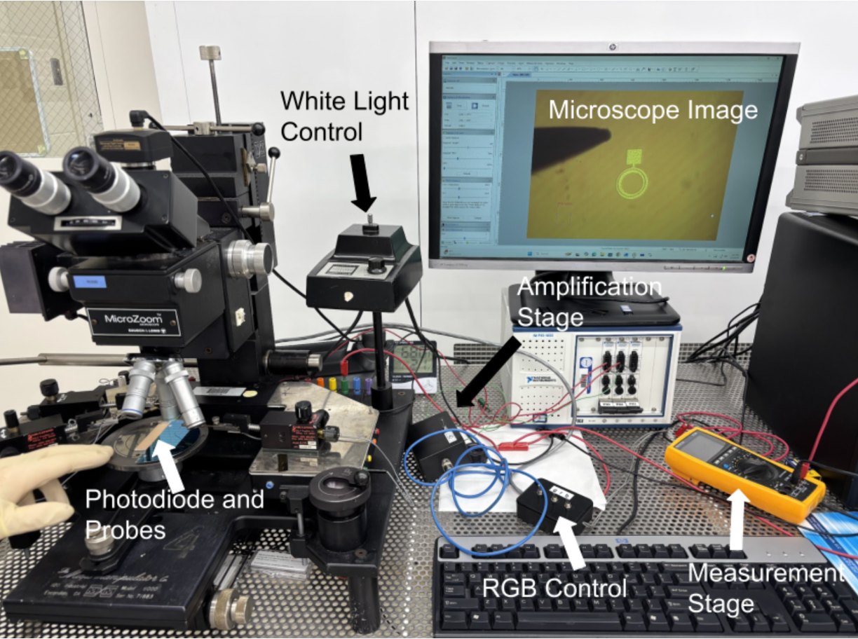 The photodiode test stand: probes on the device under the microscope, controllable white and RGB illumination, and an amplification and measurement chain.
Laser
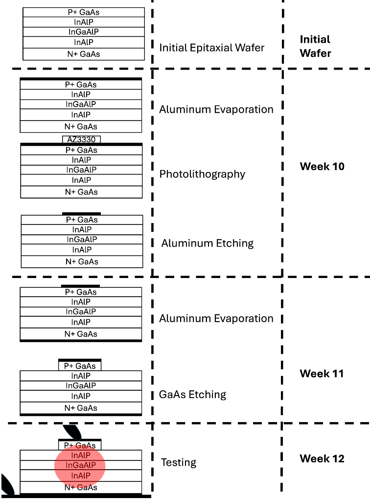
This was the part of these classes that I was the most excited for. We built a laser from a III–V epitaxial wafer, using a GaAs substrate and InGaAlP multi-quantum-well gain region, clad by InAlP optical layers. We evaporated and patterned aluminum contacts, etched the GaAs contact layer into a stripe for optical confinement, and tested the finished devices.
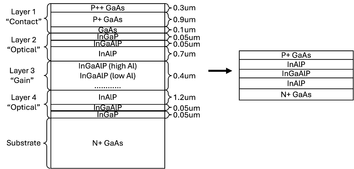 The epitaxial layer structure (left), with thicknesses, and the simplified stack used in the process diagrams (right): contact, optical cladding, gain and substrate layers.
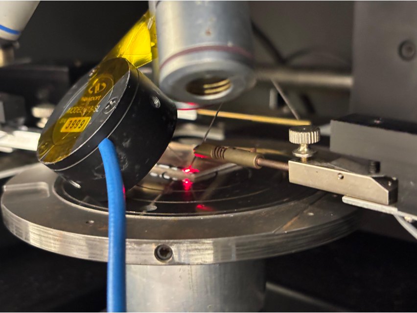
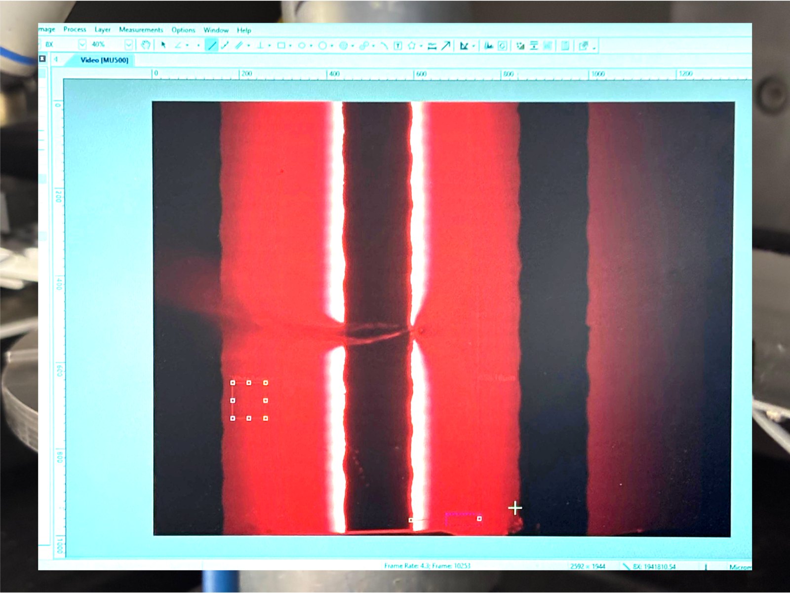
It was a little bit debatable whether or not we actually hit the lasing threshold on our device. At high current, we did start to see our emission vs current plot spike slightly, but we couldn’t push the current any higher in our setup to see if the trend continued. Regardless, this project was an incredible chance for me to see how laser diodes are actually built and operated.