Photonic Crystal Ring Resonators for Dispersion Engineering
I designed, simulated and laid out photonic crystal ring resonators, fabricated through Nokia, that use a corrugated inner wall to split chosen resonances and engineer dispersion.
- When
- Summer 2025
- Status
- Not pursued further (Q factor)
- Role
- Device design, simulation & layout
- With
- Nokia (fabrication)
Overview
This was one of my first chances to work on a research project in which I designed and fabricated my own integrated photonic structure. In our group, we have lots of students who are recruited by and work at Nokia, developing photonic chips. Working with some of these industry partners, we came up with a project that started off with a lot of steam and then hit a lot of challenges.
The initial idea was to see if we could use the same silicon process used by Nokia to do on-chip nonlinear optics. Specifically, they had a thin film of silicon nitride that theoretically had good enough confinement and a high enough third-order nonlinearity to generate a two-mode squeezed vacuum.
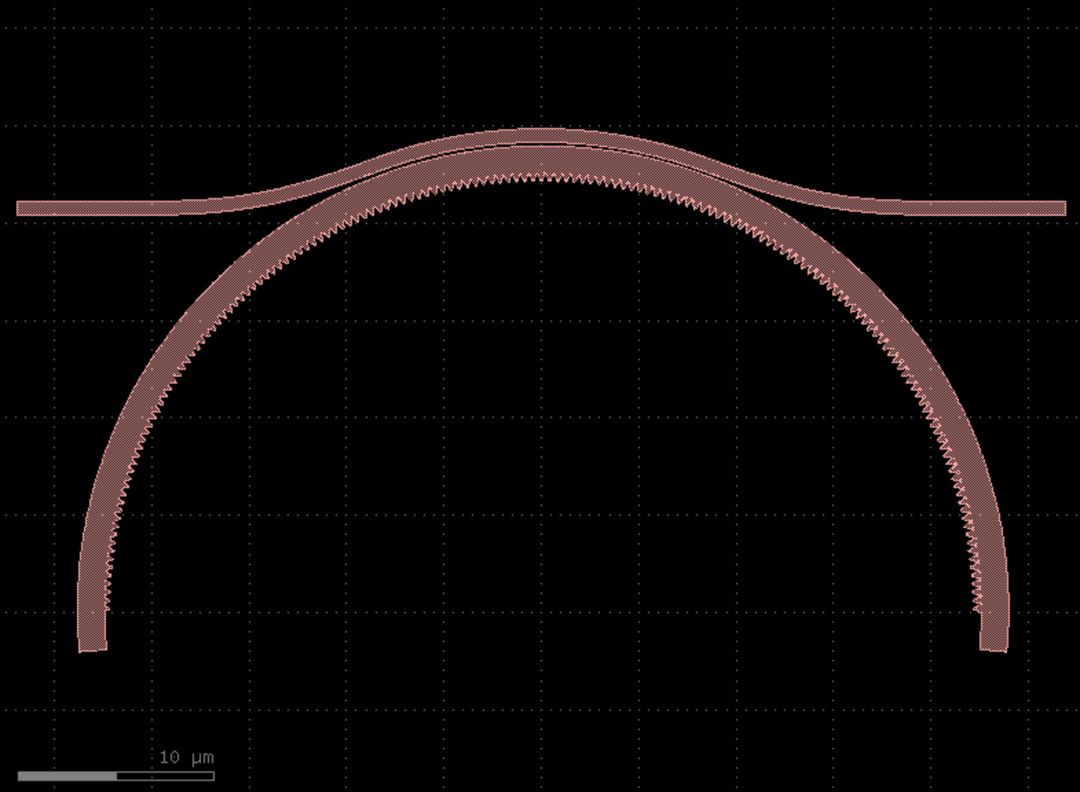
We needed anomalous dispersion in the ring in order to achieve phase matching, which was not trivial under the fabrication constraints. We actually investigated several solutions, but the most promising was using a photonic crystal ring which added a periodic corrugation of the inner wall. This would couple forward- and backward-traveling light, splitting a chosen resonance in two and giving a precise knob for controlling individual resonances and engineering the dispersion. I designed an array of these rings and had them fabricated through Nokia.
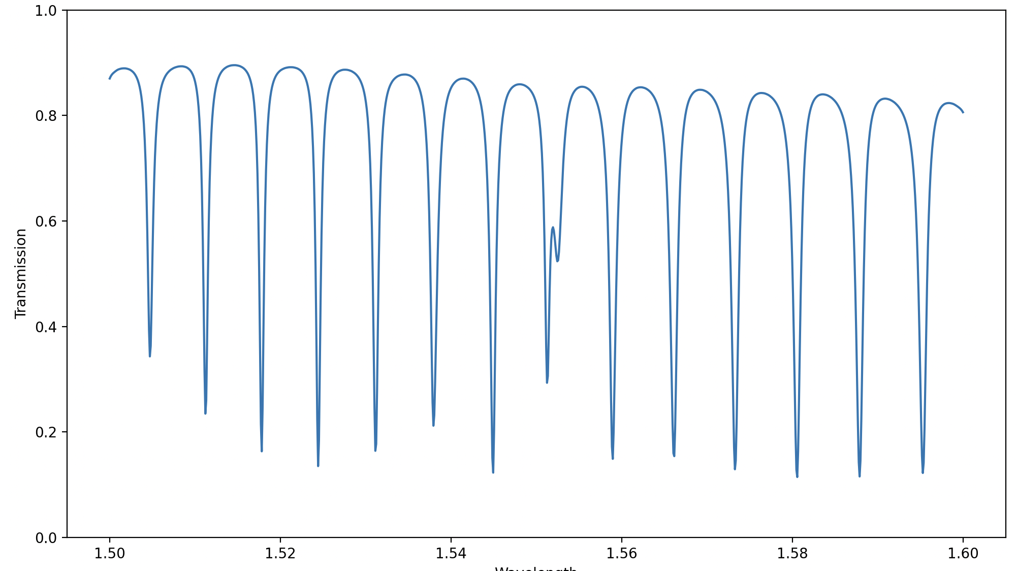 The simulated transmission spectrum. The resonances are evenly spaced except near 1.552 µm, where the corrugation splits one resonance into a doublet, exactly the targeted effect.
Design
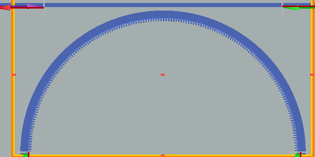
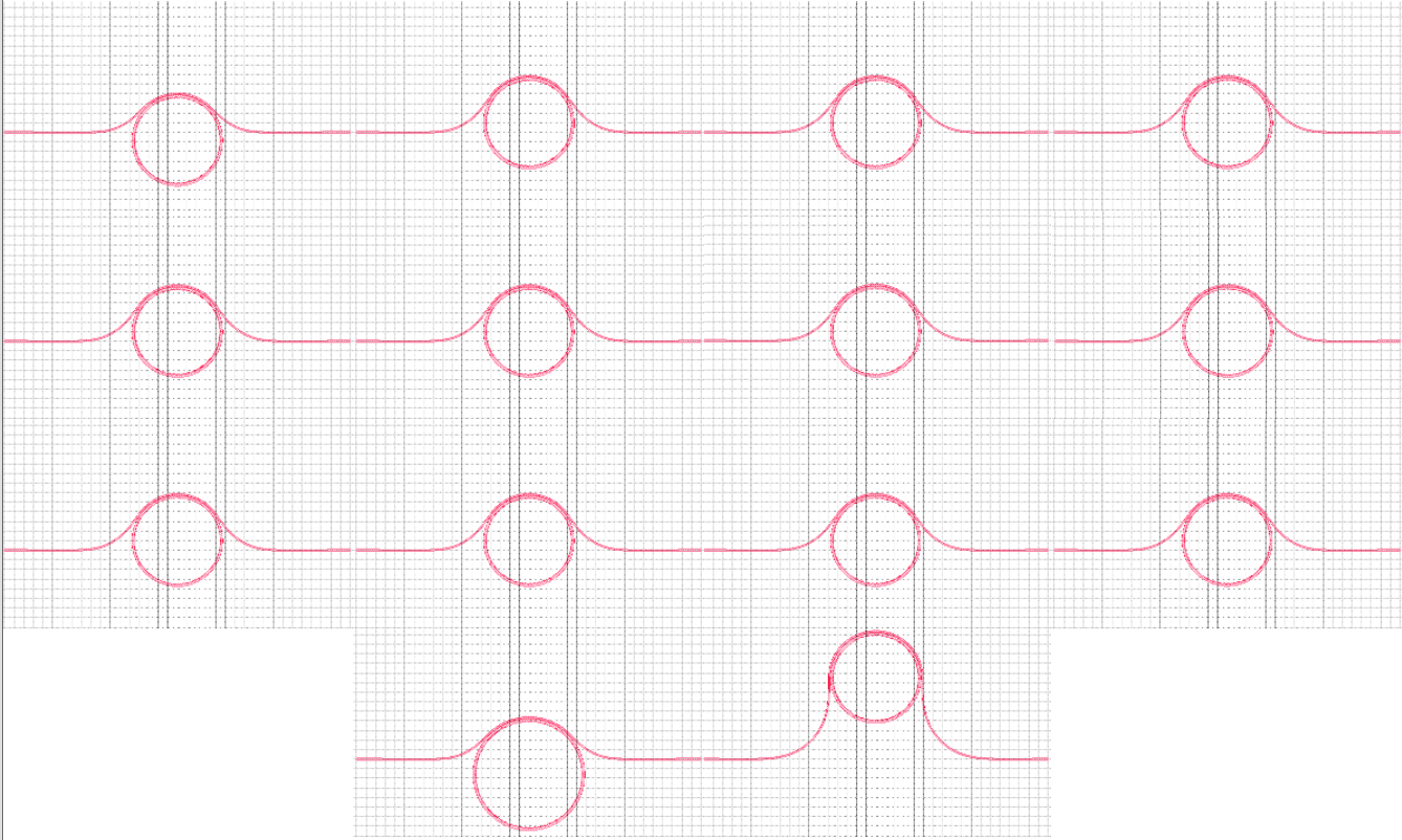
I simulated the rings in Lumerical FDTD, then laid out an array of variations for fabrication, sweeping the design parameters from ring to ring.
Outcome
The rings were fabricated and some mode splitting was observed, but after running some nonlinear optics simulations, I determined the Q-factor wouldn’t be high enough to hit the threshold power for two-mode squeezed vacuum generation.
At the same time, my boss had some new projects and opportunities coming in, and the original excitement around this project had died down. Though I spent a few months on it (and then several more months waiting for the post-fabrication data), it was also a good example of avoiding the sunk-cost fallacy. While I would love to come back to photonic crystal design in the future, I’m also grateful that I was able to move away from this when it became clear that the initial ideas would not work.