Integrated Homodyne QRNG: Chip & Deployment
Experimental work on a quantum random number generator built from a photonic chip with co-designed on-chip transimpedance amplifiers, from wirebonding the chip to deploying it at Oak Ridge National Laboratory.
- When
- 2022
- Status
- Completed
- Role
- Edge coupling, experimental work & on-site deployment
- With
- Oak Ridge National Laboratory
Overview
This was one of my first two projects in BYU’s CamachoLab, along with some FPGA work I did that tied into the same project.
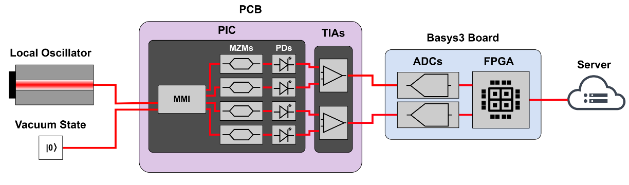
In the project I was moving into, the team had been working on doing homodyne detection of the vacuum state with record-high signal-to-noise ratios. This project co-designed a photonic chip and on-chip transimpedance amplifiers to reach that regime, and then turned the detector into a working quantum random number generator.
The Pre-existing System
When I arrived, two pieces of the system were in development and about to arrive:
- Photonic integrated circuit (PIC): the local oscillator and the vacuum input are combined in a multimode interference (MMI) coupler and split into four arms, each with a Mach–Zehnder modulator (MZM) and a photodiode. We were just about to receive this when I arrived.
- Transimpedance amplifiers (TIAs): pairs of on-chip photodiodes feed two custom TIAs which amplify the signal prior to measurement.
I had a few tasks. First of all, I was supposed to learn how to wirebond chips in BYU’s cleanroom so that I was prepared to wirebond our PICs when they arrived. Secondly, I was to work on the edge coupling setup that another student of ours had started so that we were ready to characterize the chip when it arrived. Finally, since I had some significant experience in PCB design, I was working with another student to design a secondary amplification stage on a PCB that would host the chip upon arrival (shown below).
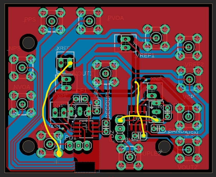 Layout of the detector’s circuit board. SMA connectors around the edge bring in the supplies, bias and reference voltages, and carry out the two amplified outputs (VOUT1, VOUT2).
This page covers the experimental side. The FPGA system and theory, which were my other main contribution, are on the QRNG FPGA Control & Randomness Extraction page.
My work
We were able to fabricate the PCB and finish the edge coupling stage. When the chip arrived, I wirebonded it in the cleanroom and spent many hours in the lab with the microscope working to align the edge couplers.
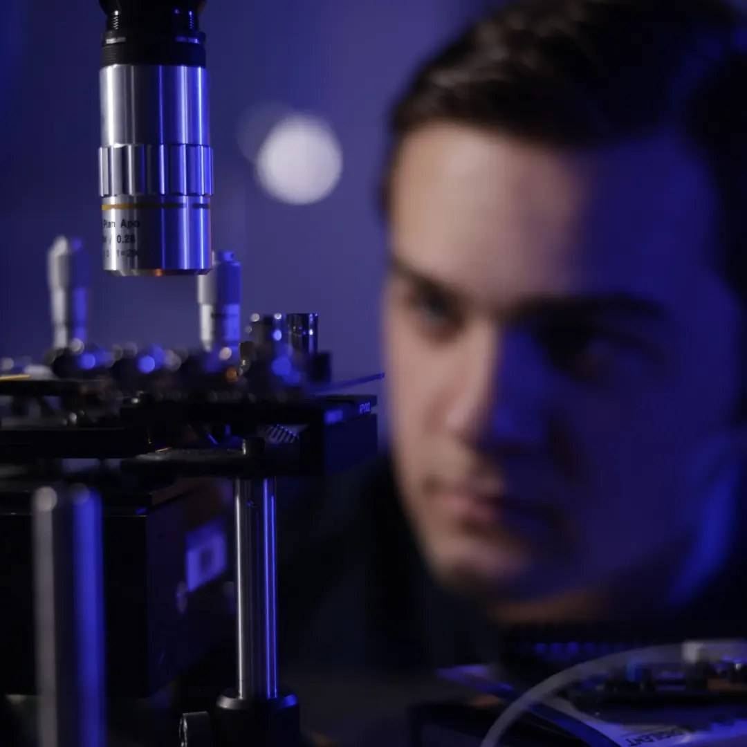
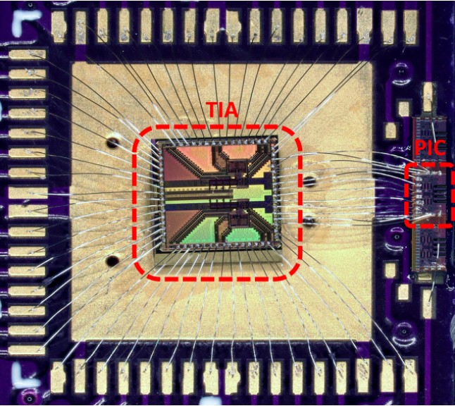
In the end, we had a working system, complete with detection, amplification, and even classical postprocessing, ready for deployment at Oak Ridge National Laboratory, which had worked with us during development so the system could be used on their QKD network.
Deployment at Oak Ridge National Laboratory
For a few months, I worked on site at ORNL. Here, I worked in a team of three from BYU to set up the same edge coupling system and the postprocessing that we had been working on during the last year. It was a great opportunity to deploy and use a real product, and a fantastic end to this project.